Everything posted by LUFER
-
How is the dry process using porous silicon?
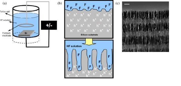
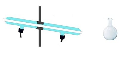
Hello, I know not really a good image, because I couldn't find a suitable one, but it was submitted that after this corrosion process it is known that you put HF and then ethanol or acetone and finish with pentane and that would be the wet concept, I just I wanted the concept of the dry process that is in the second image (dry process). If so, can you recommend some literature?
-
How is the dry process using porous silicon?
I'm having trouble finding in the literature specifically about the porous silicon process using the dry method instead of the more common wet method that is used. wet process Using porous silicon to promote wet thermal oxidation uses the process electrochemically will allow water molecules to diffuse into it. Wet oxide is often used for oxide growth. So that the structure (cavities) does not collapse after using the previously mentioned process or remove that PENTAN. Example: See the photo in attachment 01 dry process If it refers to the dry process, I can't find anything profound in the literature, it just cites the case. I would need to understand how this process works, the little I understood is that it uses two flasks where there is a cylindrical flask where there is an inlet and an outlet and the other flask where the Porous Silicon is used. If anyone can help me where I can find the literature. Example: See the photo in attachment 02
-
What is Electromagnetic Cross Section?
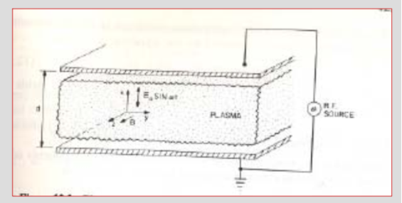
Hello, I have a question regarding the manufacturing process of electronic components in the case of the silicon deposition and corrosion process. My biggest doubt is the behavior of the plasma interacting in the reactor, I don't know if it's correct I would like someone to help me. What I understood from the subject: If you look at the image, it shows a capacitor (in the simplified case, a PECVD or RIE plasma reactor) where the particles descend from the plate and then it will collide with the particles on the bottom plate, in this case it is in the middle where the plasma wants to pass. In practice we have three directions (vectors) x, y and z, the magnetic effect occurs in the plasma where the particles have two directions or two directions in a spiral effect, so the shock is greater in the sample. In its behavior taking advantage where the field can move in the sample without having to move it. Is correct?
-
Intrinsic fermi energy of silicon: How do you find Ec and Ev?
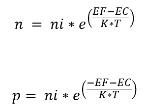
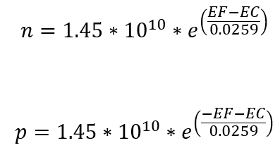
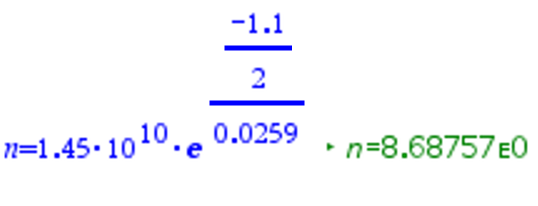
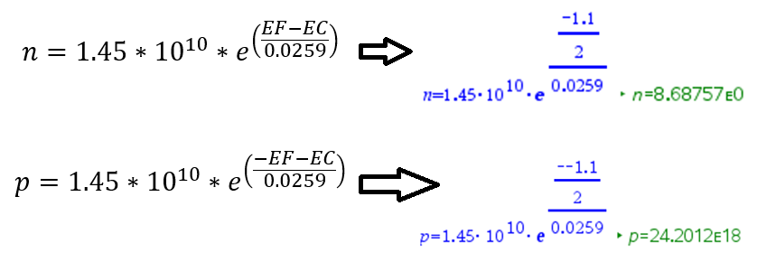
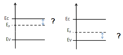
Exercise: Considering an intrinsic silicon bar at room temperature 300 K where concentration of electrons and holes with acceptor type impurities ( type P) in a concentration of 4*10^17 cm-3., q = 1.6*10^ (-19)C, kT=0.0259 eV, ni = 1.45*10^(10)cm^(-3), Eg=1.1 eV. I'm having a hard time finding Ec and Ev, if I use the equation I lack data to get this reference if I use the concept of a graph, what I need is to find the value of Ec and Ev. If I describe that Ef -Ec = - Eg/2, the values are very high there's another equation missing that I'm not able to fit here I don't know if I should be Fermi Energy, but if I insert it as a P-type material, the value is still taken
-
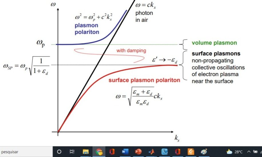
Demonstrate the graph in MATLAB referring to plasmon polariton surface
Hi I'm having difficulty with the part of inserting the graph in MATLAB using the plasmon polariton surface equations. Estou seguindo essas equações e tenho que gerar esse gráfico e não estou conseguindo alguém me orientar? Constantes %format long format short e syms m=9.11*10^(-31) % Massa do elétron - KG q=1.602*10^(-19) % Coulomb - c eo=8.8541878176*10^(-12) % Constante de permissividade do vácuo - F/m C = 300*10^6; % Velocidade da Luz em m/s n=8.45*10^(28) % n is the number of electrons (densidade do eletron) [8] oo=5.7*10^(7) % σ (COBRE)= 4.3*10^(7) condutividade (Siemens/m) = (S/m) h=6.626*10^(-34) % h constante de Planck - J⋅s pAu=((1)/(4.3*10^(7))) % Resistividade do ouro - Ω⋅m wx = linspace(1, 10000, 1E6); % Variação da Frequencia (ω) Ko=wx/C; % pagina livro (pg 40 pdf) vetor de onda da onda de propagação no vácuo Valores experimentais Ouro w=[313, 333, 357, 385, 417, 455, 500, 556, 625, 714, 833, 1000, 1250, 1430, 1670, 2000, 2500, 3330]; % Valores experimentais Ouro eps1=[36900, 33700, 30600, 27300, 24100, 20800, 17700, 14800, 12200, 9510, 7140, 5050, 3290, 2540, 1880, 1310, 839, 475]; % https://www.mathworks.com/help/matlab/ref/eps.html eps2=[25400, 21700, 18400, 15300, 12400, 9890, 7670, 5780, 4190, 2860, 1840, 1090, 568, 383, 242, 141, 72.5, 30.7]; % https://math.jhu.edu/~shiffman/370/help/techdoc/ref/eps.html Definição de Variaveis para Ouro wpAu=107.25^4;%cm-1 ωp(cm−1) IR fit [artigo optica] wtAu=2.16*10^2;%cm-1 ωτ(cm−1) IR fit [artigo optica] Definição de Variveis para Prata wpAg=7.25*10^4;%cm-1 ωp(cm−1) IR fit [artigo optica] wtAg=1.45*10^4;%cm-1 ωτ(cm−1) IR fit [artigo optica] Calculo de Permissidade da Interface 1 - Metal - Ouro e Prata (M) + Real e Im e1Au=1-((wpAu.^2)./(wx.^2+wtAu.^2)); %calculo da permissividade do Metal 1 (Au)parte real origem ε(ω)=1-((ωp)/(ω^(2))) por somou (wx.^2+wtAu) pg 31 livro e2Au=(wpAu^2.*wtAu)./(wx.^3+wx.*wtAu.^2); %calculo da permissividade do Metal 1 (Au) parte imaginaria ω(ε)=((ωp^(2)*τ)/(ω+ω^(3)*τ^(2))) E1Au= e1Au + e2Au*i; %Permissividade da interface 1 - Au (metal) e1Ag=1-((wpAg.^2)./(wx.^2+wtAg.^2));% calculo da permissividade do Metal 1 (Ag)parte real origem ε(ω)=1-((ωp)/(ω^(2))) por somou (wx.^2+wrAu) pg 31 livro e2Ag=(wpAg^2.*wtAg)./(wx.^3+wx.*wtAg.^2);% calculo da permissividade do Metal 1 (Ag) parte imaginaria ω(ε)=((ωp^(2)*τ)/(ω+ω^(3)*τ^(2))) E1Ag= e1Ag + e2Ag*i;% Permissividade da interface 1 - Au (metal) Calculo da Permissividade da Interface 2 - Eletrolitico (I) E2ar=1; %Permissividade constante Ar [] E2silicio=1.45;%Permissividade constante Oxido de Silicio [https://www.nature.com/articles/s41598-019-38859-2]+ E2=1;%Permissividade da interface 2 - Ar (dieletrico) Calculo de Fator de Dispersao do Au / Silicio Relação de dispersão dos SPPs propagando-se na interface entre os dois meios-espaços. (pg 44) BAuSi=Ko*sqrt((E1Au*E2silicio)/(E1Au+E2silicio)); % B=Ko*√(((ε1*ε2)/(ε1+ε2))) BAuSireal=exp (real(BAuSi)*1000000/4); % Hy(z) = A2*e^(i*β*x)*e^(−k2*z) Calculo de Fator de Dispersao do Ag / Ar e Au / Ar BAgAr=Ko*sqrt((E1Ag*E2ar)/(E1Ag+E2ar)); % B=Ko*√(((ε1*ε2)/(ε1+ε2))) BAgAr_real=exp (real(BAgAr)*10^(6)); % Hy(z) = A2*e^(i*β*x)*e^(−k2*z) BAuAr=Ko*sqrt((E1Au*E2ar)/(E1Au+E2ar)); % B=Ko*√(((ε1*ε2)/(ε1+ε2))) BAuArreal=exp (real(BAuAr)*1000000/4); % % Hy(z) = A2*e^(i*β*x)*e^(−k2*z) mesmo ω final ranger do wx Calculo de Fator de Dispersao do Ag / Silicio BAgSi=Ko*sqrt((E1Ag*E2silicio)/(E1Ag+E2silicio)); % B=Ko*√(((ε1*ε2)/(ε1+ε2))) BAgSi_real = exp (real (BAgSi) * 1000000); %% Hy (z) = A2 * e ^ (i * β * x) * e ^ (- k2 * z) Permissividade em gráfico plot (BAuArreal, wx, BAuSireal, wx, BAgAr_real, wx, BAgSi_real, wx, Beta_Au_Ar, wx); título ('Interface'); ylabel ('frequencia em {\ omega} e plasmo {\ omega} p (cm ^ - ^ 1)'); xlabel ('vetor de onda {\ beta} (100) m ^ - ^ 1'); eixo ([1 100000 1 100000]); set (gca, 'XScale', 'log', 'YScale', 'log'); grade de legenda ('Ouro / Ar', 'Ouro / Si', 'Prata / Ar', 'Prata / Si', 'Beta_Au_Ar')
-
Plasmonic - Dielectric function
Regarding the electrical permittivity of the metal in a high frequency regime, I cannot find research material related to the lead dielectric function (PD). I can't get the matatrial as values, I'll let you comment on that. I know that Pd can inhibit the amount of gamma rays in the x-ray case, but I would like to know about values related to that.
-
PLASMONICS - Exercise
Hi I'm having difficulties with the plasmonica exercise, I sell some books and scientific publications I came across that there are two or more ways to get the result but I don't know what the correct sequence is. Values: τ, γ and mainly ωp^(2). ωp^(2)= in most of the literature = Design and Application of Plasmonic Devices - A Thesis and PLASMONICS: FUNDAMENTALS AND APPLICATIONS - STEFAN A. MAIER And research I found that gets confusing: https://www.osapublishing.org/ao/fulltext.cfm?uri=ao-22-7-1099&id=26571 Hi I'm having difficulties with the plasmonica exercise, I sell some books and scientific publications I came across that there are two or more ways to get the result but I don't know what the correct sequence is. Values: τ, γ and mainly ωp^(2). ωp^(2)= in most of the literature = Design and Application of Plasmonic Devices - A Thesis and PLASMONICS: FUNDAMENTALS AND APPLICATIONS - STEFAN A. MAIER And research I found that gets confusing: https://www.osapublishing.org/ao/fulltext.cfm?uri=ao-22-7-1099&id=26571 Here is the question of the exercise, resolution and research material. Obtain an expression for the electrical permittivity of a metal ε(ω) in the low-frequency regime in the free electron model. Using this expression determine the electrical permittivity of Au, Ag and Cu for a frequency of 10 GHz (microwave region). Tip get the necessary parameters for calculations from reported literature. Souce https://core.ac.uk/download/pdf/190334041.pdf https://www.springer.com/gp/book/9780387331508 EX1.pdf
-
Unfolding the energy levels of the nd1 Valencia electron of an atom subjected to a crystalline field of tetrahedral symmetry.
my difficulty is related to: (nd1) and (d) not the same thing, or have different meanings? Found nothing about (nd1) .
-
Unfolding the energy levels of the nd1 Valencia electron of an atom subjected to a crystalline field of tetrahedral symmetry.
Livro_Quimica_Quimica Inorganica II.ind On pages 85, 88, 93, 94. Electronic Structure and Properties of Transition Metal Compounds, Second Edition (teacher's book). Page 89 https://www.bdtd.uerj.br:8443/bitstream/1/12871/1/Tese_Ludiane.pdf page 21 onwards
-
Unfolding the energy levels of the nd1 Valencia electron of an atom subjected to a crystalline field of tetrahedral symmetry.
I'm having trouble understanding an excerpt of the question. Whether there is a deep meaning (nd1). I adopted it as valence d to answer the question. See my answer in the attachment. I would like to understand nd1. help.docx
-
Wavefunction Equations Of Hybridized Orbitals
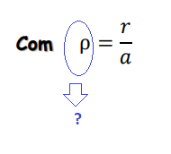
but sorry, do you have the p-value? I don't know if translation fails. r i know the radius, but the p don't know. I don't know if it's constant.
-
Wavefunction Equations Of Hybridized Orbitals
Because I'm asking about p, I think it's a constant. That I have neither p-value nor r-value.
-
Wavefunction Equations Of Hybridized Orbitals
-
Wavefunction Equations Of Hybridized Orbitals
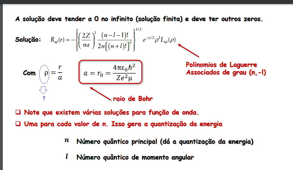
Hello after having done a search if I can find the equations and I'll give you their source. The only thing I couldn't find was this one in the annex. Please help me know what this value or name is. https://www.clutchprep.com/chemistry/practice-problems/143395/the-s-orbital-is-spherical-nondirectional-because-check-all-that-apply-a-the-ang https://www.learnpick.in/prime/documents/ppts/details/4225/atomic-structure-and-quantum-numbers https://slideplayer.com.br/slide/1595583/ http://www.ensinoadistancia.pro.br/ead/qg/aula-7/aula-7.html https://pbs.twimg.com/media/EWxsOfKWoAIk6eq?format=jpg&name=large https://web1.eng.famu.fsu.edu/~dommelen/quantum/style_a/hyd.html ρ=r/α ?
-
Wavefunction Equations Of Hybridized Orbitals
Exactly the algebraic expression for each case, that way I can generate the graph in matlab. I'm having to simulate, but lacking data in the equations.
-
Wavefunction Equations Of Hybridized Orbitals
Hi, I'm looking for the equations to perform the wave function of the orbitals, that way I can give a graph. The problem I only encounter situations in basic energy transfer (valence).And also Schrodinger's theory for obtaining energy levels. Task: Make wavefunctions of the sp2, sp3, sd3 hybridized orbitals respectively. I need the wavefunction equations for the hybridized orbitals.

